The Impact of Solvent Vapor on the Film Morphology and Crystallization Kinetics of Lead Halide Perovskites during Annealing

Yu Zhong, Dominik Seeberger, Eva M. Herzig, Anna Köhler, Fabian Panzer, Cheng Li and Sven Huettner

ACS Appl. Mater. Interfaces 13 (2021) 45365–45374

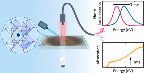
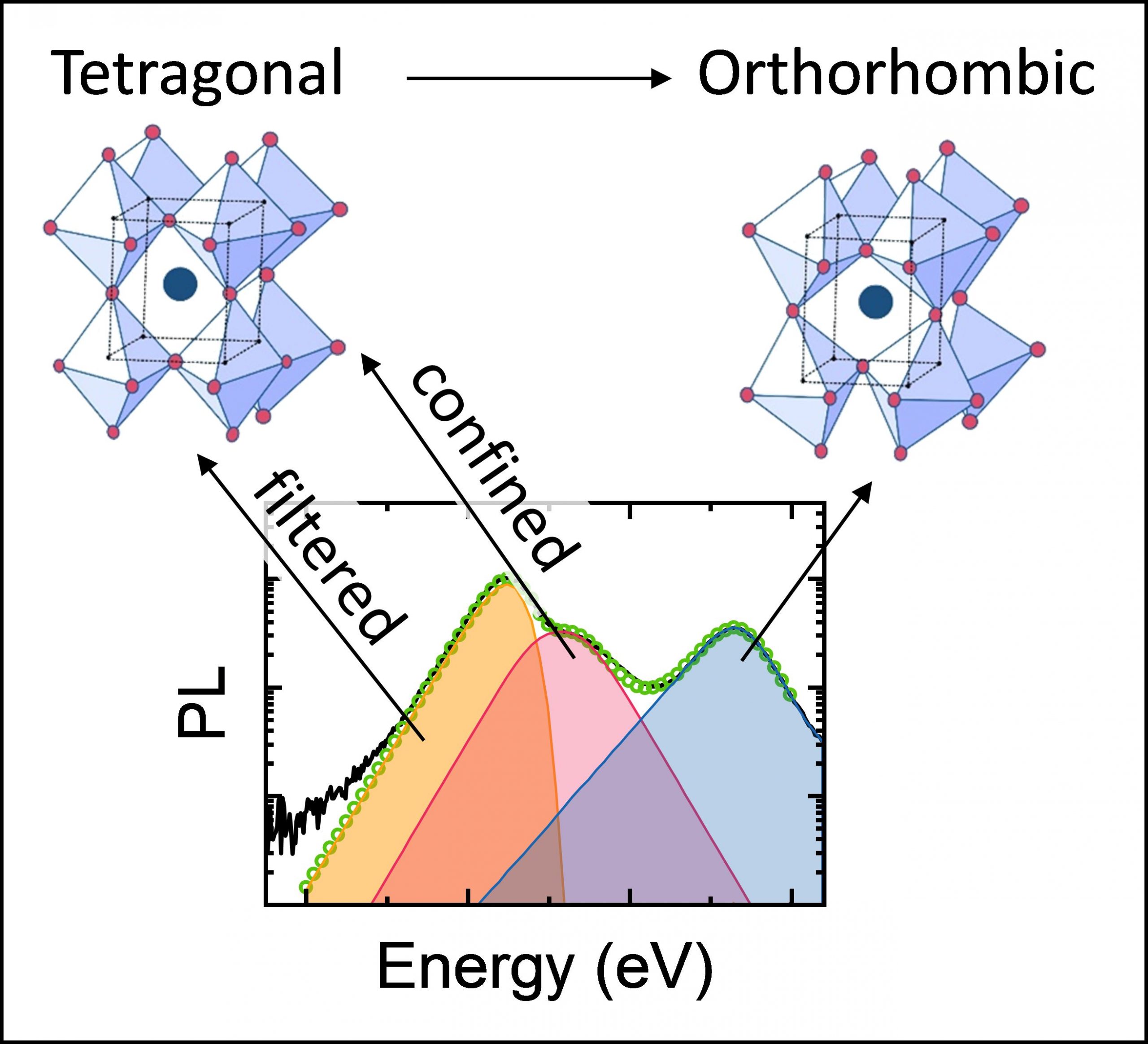
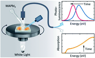
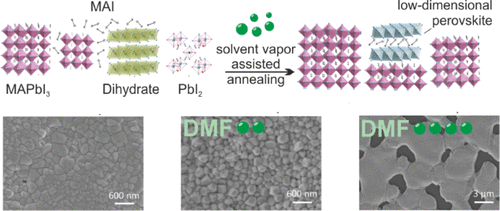
One of the key factors for the remarkable improvements of halide perovskite solar cells over the last few years is the increased control over perovskite crystallinity and its thin film morphology. Among various processing methods, solvent vapor-assisted annealing (SVAA) has proven to be promising in achieving high-quality perovskite films. However, a comprehensive understanding of the perovskite crystallization process during SVAA is still lacking. In this work, we use a home-built setup to precisely control the SVAA conditions to investigate in detail the perovskite crystallization kinetics. By changing the solvent vapor concentration during annealing, the perovskite grain size can be tuned from 200 nm to several micrometers. We monitor the crystallization kinetics during solvent-free annealing and SVAA using in situ grazing incidence wide-angle X-ray scattering, where we find a diminished perovskite growth rate and the formation of low dimensional perovskite at the top of the perovskite layer during SVAA. Scanning electron microscopy images of the final films further suggest that the perovskite growth follows an Ostwald ripening process at higher solvent concentrations. Thus, our results will contribute to achieve a more targeted processing of perovskite films.

Understanding Differences in the Crystallization Kinetics between One-Step Slot-Die Coating and Spin Coating of MAPbI3 Using Multimodal In Situ Optical Spectroscopy

Konstantin Schötz, Christopher Greve, Arjan Langen, Harrie Gorter, Ilker Dogan, Yulia Galagan, Albert J. J. M. van Breemen, Gerwin H. Gelinck, Eva M. Herzig, Fabian Panzer

Adv. Optical Mater. (2021) 2101161

To develop a detailed understanding about halide perovskite processing from solution, the crystallization processes are investigated during spin coating and slot-die coating of MAPbI3 at different evaporation rates by simultaneous in situ photoluminescence, light scattering, and absorption measurements. Based on the time evolution of the optical parameters it is found that for both processing methods initially solvent-complex-structures form, followed by perovskite crystallization. The latter proceeds in two stages for spin coating, while for slot-die coating only one perovskite crystallization phase occurs. For both processing methods, it is found that with increasing evaporation rates, the crystallization kinetics of the solvent-complex structure and the perovskite crystallization remain constant on a relative time scale, whereas the duration of the second perovskite crystallization in spin coating increases. This second perovskite crystallization appears restricted due to differences in solvent-complex phase morphologies from which the perovskite forms. The work emphasizes the importance of the exact precursor state properties on the perovskite formation. It further demonstrates that detailed analyses of multimodal optical in situ spectroscopy allows gaining a fundamental understanding of the crystallization processes that take place during solution processing of halide perovskites, independent from the specific processing method.

Electrical conductivity of halide perovskites follows expectations from classical defect chemistry

Nico Leupold, Anna Lena Seibel, Prof. Dr. Ralf Moos and Dr. Fabian Panzer

Eur. J. Inorg. Chem. (2021) 2882 –2889

Defect chemistry is key to understand electrical properties of many functional materials including halide perovskites. However, expectations from defect chemistry about the dependency of defect densities on the doping regime of halide perovskites have not yet been clearly confirmed experimentally. Here, we measure the electrical conductivity of the model halide perovskite Methylammonium Lead Iodide over a wide range of iodine partial pressures. We find that with iodine partial pressure the electrical conductivity changes with different slopes in a double-logarithmic representation, indicating changes of the perovskite conductivity mechanism. Considering differences in the mobilities of the various defect species, we derive expectations about the dependence of the total conductivity of the perovskite as a function of iodine partial pressure. We find iodine vacancies dominating the conductivity at low iodine partial pressures, whereas at higher partial pressures holes govern the total conductivity. We find the concentration of iodide vacancies to be ∼1018 cm−3, in good agreement with the expected values based on intrinsic ionic disorder. Finally, for the case that the intrinsic ionic disorder concentration is overestimated, we elucidate the possibility to explain the conductivity profile by impurity induced acceptor doping in the perovskite. Thus, our work will allow to develop a more fundamental understanding about the electrical properties of halide perovskites.

Suppressed ion migration in powder-based perovskite thick films using an ionic liquid

Phillipp Ramming, Nico Leupold, Konstantin Schötz, Anna Köhler, Ralf Moos, Helen Grüninger and Fabian Panzer

J. Mater. Chem. C, (2021) 9 11287-11837

While solution-processed halide perovskite thin films caused enormous attention when used in solar cells, thick films prepared by compressing perovskite powders are considered promising candidates for the next generation of X-ray detectors. However, X-ray detectors based on such powder-pressed perovskites typically suffer from relatively high dark currents, which were attributed to be caused by ion migration. Here we show that the dark current in 800 μm thick powder-pressed MAPbI3-pellets can be reduced by a factor of 25 when using a passivated powder. The passivation was achieved by adding 1 mol% of the ionic liquid (IL) BMIMBF4 to the precursors MAI and PbI2 during the mechanochemical synthesis of the MAPbI3 powder. NMR verified the presence of the IL, and its impact on the excited state recombination dynamics was manifested in an increase in the photoluminescence (PL) intensity and a decrease in the monomolecular (trap-assisted) recombination rate, both by about one order of magnitude. By measuring the migration of a PL quenching front upon application of an electric field in a microscope, we determine an ionic diffusivity in the typical range of iodide vacancies in the non-passivated pellet. At the same time, we observe no such PL quenching front in the passivated pellet. Concomitantly, dark I–V curves are hysteresis-free, and light-soaking effects are absent, in contrast to non-passivated pellets. Thus, our work demonstrates the effect on the optical and electrical properties when passivating mechanochemically synthesized halide perovskite powders using an IL, which will facilitate the further development of powder-based perovskite X-ray detectors.

How antisolvent miscibility affects perovskite film wrinkling and photovoltaic properties

Seul-Gi Kim, Jeong-Hyeon Kim, Philipp Ramming, Yu Zhong, Konstantin Schötz, Seok Joon Kwon, Sven Huettner, Fabian Panzer and Nam-Gyu Park

Nature Communications (2021) 1554

Charge carriers’ density, their lifetime, mobility, and the existence of trap states are strongly affected by the microscopic morphologies of perovskite films, and have a direct influence on the photovoltaic performance. Here, we report on micro-wrinkled perovskite layers to enhance photocarrier transport performances. By utilizing temperature-dependent miscibility of dimethyl sulfoxide with diethyl ether, the geometry of the microscopic wrinkles of the perovskite films are controlled. Wrinkling is pronounced as temperature of diethyl ether (TDE) decreases due to the compressive stress relaxation of the thin rigid film-capped viscoelastic layer. Time-correlated single-photon counting reveals longer carrier lifetime at the hill sites than at the valley sites. The wrinkled morphology formed at TDE = 5 °C shows higher power conversion efficiency (PCE) and better stability than the flat one formed at TDE = 30 °C. Interfacial and additive engineering improve further PCE to 23.02%. This study provides important insight into correlation between lattice strain and carrier properties in perovskite photovoltaics.

Using In Situ Optical Spectroscopy to Elucidate Film Formation of Metal Halide Perovskites

Konstantin Schötz and Fabian Panzer

J. Phys. Chem. A (2021)

The research interest in halide perovskites has gained momentum enormously over the last recent years, also due to the demonstration of high-efficient perovskite-based optoelectronic devices. A prerequisite for such highly efficient devices is to realize high-quality perovskite layers, which requires a deep understanding about the perovskite formation and good process control. In that context, in situ optical spectroscopy during the processing of halide perovskites has become increasingly popular. Even though it is a relatively easily accessible yet powerful tool for studying perovskite formation, there exist some technical and analytical aspects that need to be considered to unfold its full potential. In this Perspective, we give an overview of the latest developments in the field of in situ optical spectroscopy to control and better understand the film processing of halide perovskites. We highlight possibilities and pitfalls regarding the analysis of measured optical data, discuss the development of technical concepts, and address future prospects of optical in situ spectroscopy.

Structural Diversity in Layered Hybrid Perovskites, A2PbBr4 or AA′PbBr4, Templated by Small Disc-Shaped Amines

Yuan-Yuan Guo, Lin-Jie Yang, Simon Biberger, Jason A. McNulty, Teng Li, Konstantin Schötz, Fabian Panzer and Philip Lightfoot

Inorg. Chem. 59 (2020) 12858–12866

We present three new hybrid layered lead(II) bromide perovskites of generic composition A2PbBr4 or AA′PbBr4 that exhibit three distinct structure types. [TzH]2PbBr4 ([TzH+] = 1,2,4-triazolium) adopts a (001)-oriented layer structure and [AaH]2PbBr4, ([AaH+] = acetamidinium) adopts a (110)-oriented type, whereas [ImH][TzH]PbBr4, ([ImH+] = imidazolium) adopts a rare (110)-oriented structure with enhanced corrugation (i.e., 3 × 3 type). The crystal structures of each are discussed in terms of the differing nature of the templating molecular species. Photoluminescent spectra for each are reported and the behaviors discussed in relation to the different structure of each composition.

Investigating the Tetragonal-to-Orthorhombic Phase Transition of Methylammonium Lead Iodide Single Crystals by Detailed Photoluminescence Analysis

Konstantin Schötz, Abdelrahman M. Askar, Anna Köhler, Karthik Shankar and Fabian Panzer

Adv. Optical Mater. (2020) 2000455

Here, the phase‐transition from tetragonal to orthorhombic crystal structure of the halide perovskite methylammonium lead iodide single crystal is investigated. Temperature dependent photoluminescence (PL) measurements in the temperature range between 165 and 100 K show complex PL spectra where in total five different PL peaks can be identified. All observed PL features can be assigned to different optical effects from the two crystal phases using detailed PL analyses. This allows to quantify the fraction of tetragonal phase that still occurs below the phase transition temperature. It is found that at 150 K, 0.015% tetragonal phase remain, and PL signatures are observed from quantum confined tetragonal domains, suggesting their size to be about 7–15 nm down to 120 K. The tetragonal inclusions also exhibit an increased Urbach Energy, implying a high degree of structural disorder. The results first illustrate how a careful analysis of the PL can serve to deduce structural information, and second, how structural deviations in halide perovskites have a significant impact on the optoelectronic properties of this promising class of semiconductors.

Investigating two-step MAPbI3 thin film formation during spin coating by simultaneous in situ absorption and photoluminescence spectroscopy

Mihirsinh Chauhan, Yu Zhong, Konstantin Schötz, Brijesh Tripathi, Anna Köhler, Sven Huettner and Fabian Panzer

J. Mater. Chem. A, 8 (2020) 5086-5094

To date, the two-step processing method represents an attractive route for the thin film formation of halide perovskites. However, a fundamental understanding of the film formation dynamics in the case of spin coating methylammonium iodide (MAI) on PbI2 has not been established yet. Here we apply in situ optical spectroscopy during the two-step film formation of the model halide perovskite MAPbI3 via spin coating. We identify and analyze in detail the optical features that occur in the photoluminescence and the corresponding absorption spectra during processing. We find that the film formation takes place in five consecutive steps, including the formation of a MAPbI3 capping layer via an interface crystallization and the occurrence of an intense dissolution–recrystallization process. Consideration of confinement and self-absorption effects in the PL spectra, together with consideration of the corresponding absorption spectra allows quantification of the growth rate of the initial interface crystallization, which is found to be 11 nm s−1 under our processing conditions. We find that the main dissolution–recrystallization process happens at a rate of 445 nm s−1, emphasizing its importance to the overall processing.

Double peak emission in lead halide perovskites by self-absorption

Konstantin Schötz, Abdelrahman M. Askar, Wei Peng, Dominik Seeberger, Tanaji P. Gujar, Mukundan Thelakkat, Anna Köhler, Sven Huettner, Osman M. Bakr, Karthik Shankar and Fabian Panzer

J. Mater. Chem. C 8 (2020) 2289-2300

Despite the rapidly increasing efficiencies of perovskite solar cells, the optoelectronic properties of this material class are not completely understood. Especially when measured photoluminescence (PL) spectra consist of multiple peaks, their origin is still debated. In this work, we investigate in detail double peak PL spectra of halide perovskite thin films and single crystals with different material compositions. By different optical spectroscopic approaches and quantitative models, we demonstrate that the additional PL peak results from an extensive self-absorption effect, whose impact is intensified by strong internal reflections. This self-absorption accounts for the unusual temperature dependence of the additional PL peak and it implies that absorption until far into the perovskite’s Urbach tail is important. The internal reflections entail that even for thin films self-absorption can have a significant contribution to the PL spectrum. Our results allow for a clear assignment of the PL peaks by differentiating between optical effects and electronic transitions, which is a necessary requirement for understanding the optoelectronic properties of halide perovskites.

Impact of excess PbI2 on the structure and the temperature dependent optical properties of methylammonium lead iodide perovskites

Tobias Meier, Tanaji P. Gujar, Andreas Schönleber, Selina Olthof, Klaus Meerholz, Sander van Smaalen, Fabian Panzer, Mukundan Thelakkat and Anna Köhler

J. Mater. Chem. C 6 (2018) 7512-7519

We investigate the impact of excess PbI2 in the precursor solution on the structural and optical properties of thin films of the model hybrid perovskite methylammonium lead iodide (MAPbI3). We find that excess of PbI2 in the precursor solution results in crystalline PbI2 in the final thin film that is located at the grain boundaries. From UPS we find that this crystalline PbI2 phase has no direct impact on the electronic structure of MAPbI3. In contrast to this, temperature dependent absorption measurements indicate a systematic change in the temperature dependence of the exciton binding energy in the perovskite. We also observe a decrease in the critical temperature and a concomitant smearing out of the tetragonal–orthorhombic phase transition as a function of excess PbI2. Our results thus help to better understand the exact role of PbI2 in the perovskite layer and pave the way for a more tailored design of perovskite solar cells.

The role of PbI2 in CH3NH3PbI3 perovskite stability, solar cell parameters and device degradation

Tanaji P. Gujar, Thomas Unger, Andreas Schönleber, Martina Fried, Fabian Panzer, Sander van Smaalen, Anna Köhler and Mukundan Thelakkat

Phys. Chem. Chem. Phys., 20 (2018) 605-614

We report a systematic investigation on the role of excess PbI2 content in CH3NH3PbI3 perovskite film properties, solar cell parameters and device storage stability. We used the CH3NH3I vapor assisted method for the preparation of PbI2-free CH3NH3PbI3 films under a N2 atmosphere. These pristine CH3NH3PbI3 films were annealed at 165 °C for different time intervals in a N2 atmosphere to generate additional PbI2 in these films. From XRD measurements, the excess of PbI2 was quantified. Detailed characterization using scanning electron microscopy, X-ray diffraction, UV-Visible and photoluminescence for continuous aging of CH3NH3PbI3 films under ambient condition (50% humidity) is carried out for understanding the influence of different PbI2 contents on degradation of the CH3NH3PbI3 films. We find that the rate of degradation of CH3NH3PbI3 is accelerated due to the amount of PbI2 present in the film. A comparison of solar cell parameters of devices prepared using CH3NH3PbI3 samples having different PbI2 contents reveals a strong influence on the current density–voltage hysteresis as well as storage stability. We demonstrate that CH3NH3PbI3 devices do not require any residual PbI2 for a high performance. Moreover, a small amount of excess PbI2, which improves the initial performance of the devices slightly, has undesirable effects on the CH3NH3PbI3 film stability as well as on device hysteresis and stability.

Impact of Structural Dynamics on the Optical Properties of Methylammonium Lead Iodide Perovskites

Fabian Panzer, Cheng Li, Tobias Meier, Anna Köhler and Sven Huettner

Adv. Energy Mater. 19 (2017) 1700286

Organolead halide perovskites have attracted a lot of attention over the recent years mostly due to their bright prospective application in photovoltaic devices. For further development, characterization of their physical properties plays a seminal role in order to gain an in-depth understanding of these mid-bandgap ionic semiconductors. Their unique optical and electronic properties are a result of their characteristic electronic structure. Temperature dependent optical spectroscopy, i.e., absorption and photoluminescence (PL) characterization, gives access to their electronic nature that draws strong correlations to their structural properties. Those properties include static and dynamic disorder, and defects or phase transitions, which will be demonstrated in the first part of this research view. The second part focuses on ion migration in these hybrid semiconductors, which can strongly affect the slow dynamics of optical properties. Light-activated ions result in a number of complex processes that can lead to an increase, but also a decrease of PL intensity, or induce PL intermittency. Parameters like light intensity, crystal quality, and defect density all influence these processes, and ultimately the electronic nature of the hybrid perovskites. We will briefly summarize current achievements and point out challenges for upcoming research.

Effect of Thermal and Structural Disorder on the Electronic Structure of Hybrid Perovskite Semiconductor CH3NH3PbI3

Shivam Singh, Cheng Li, Fabian Panzer, K. L. Narasimhan, Anna Graeser, Tanaji P. Gujar, Anna Köhler, Mukundan Thelakkat, Sven Huettner and Dinesh Kabra

J. Phys. Chem. Lett. 7 (2016) 3014–3021

In this Letter, we investigate the temperature dependence of the optical properties of methylammonium lead iodide (MAPbI3 = CH3NH3PbI3) from room temperature to 6 K. In both the tetragonal (T > 163 K) and the orthorhombic (T < 163 K) phases of MAPbI3, the band gap (from both absorption and photoluminescence (PL) measurements) decreases with decrease in temperature, in contrast to what is normally seen for many inorganic semiconductors, such as Si, GaAs, GaN, etc. We show that in the perovskites reported here, the temperature coefficient of thermal expansion is large and accounts for the positive temperature coefficient of the band gap. A detailed analysis of the exciton line width allows us to distinguish between static and dynamic disorder. The low-energy tail of the exciton absorption is reminiscent of Urbach absorption. The Urbach energy is a measure of the disorder, which is modeled using thermal and static disorder for both the phases separately. The static disorder component, manifested in the exciton line width at low temperature, is small. Above 60 K, thermal disorder increases the line width. Both these features are a measure of the high crystal quality and low disorder of the perovskite films even though they are produced from solution.

Reversible Laser Induced Amplified Spontaneous Emission from Coexisting Tetragonal and Orthorhombic Phases in Hybrid Lead Halide Perovskites

Fabian Panzer, Sebastian Baderschneider, Tanaji P. Gujar, Thomas Unger, Sergey Bagnich, Marius Jakoby, Heinz Bässler, Sven Hüttner, Jürgen Köhler, Ralf Moos, Mukundan Thelakkat, Richard Hildner and Anna Köhler

Adv. Optical Mater. 6 (2016) 917-928

The photoluminescence in a lead halide perovskite is measured for different temperatures (5–300 K) and excitation fluences (21–1615 μJ cm−2). It is found that amplified spontaneous emission (ASE) is observed for an excitation density larger than about 1 × 1018 cm−3 for both the tetragonal phase above 163 K and the orthorhombic phase below about 163 K. The fluence that is required to obtain this excitation density depends on temperature and phase since the nonradiative decay of excitations is temperature activated with different activation energies of inline image and inline image for the tetragonal and orthorhombic phase, respectively. The ASE from the tetragonal phase—usually prevailing at temperatures above about 163 K—can also be observed at 5 K, in addition to the ASE from the orthorhombic phase, when the sample is previously exposed to a fluence exceeding 630 μJ cm−2 at a photon energy of 3.68 eV. This additional ASE can be removed by mild heating to 35 K or optically, by exposing the sample by typically a few seconds with a fluence around 630 μJ cm−2. The physical mechanism underlying this optically induced phase transition process is discussed. It is demonstrated that this phase change can, in principle, be used for an all-optical “write–read–erase” memory device.